ANNOUNCEMENTS


NIST UNIVERSITY
Institute Park, Berhampur, Odisha-761008, India

 (1)-Photoroom.png "For engineering and management programs")
Educate & train the students to have in-depth knowledge of the subjects in the field of Electronics and Communication Engineering thereby making them develop confidence for R & D activities and placement in multinational and national companies so that the students will be of immediate use to industry, nation and mankind.
Progressively achieve higher levels of quality standards by adopting latest learning / teaching processes which are embedded in the support system and to maintain an environment which fosters holistic development and strengthens the morality & ethics of the learners. Electronics and communication department is known as a cutting edge department for VLSI, Semiconductor Devices, 3G-4G communication and microwave research. Apart from that it is a great place for teaching and learning at the undergraduate and graduate level.
22 Students have cleared the level-5 of ESSCI Certification exam from the first batch out of 36 registered students.
3G/
4G
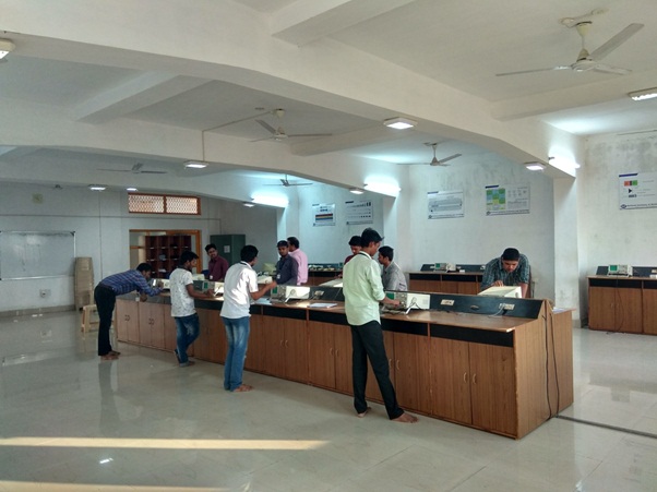
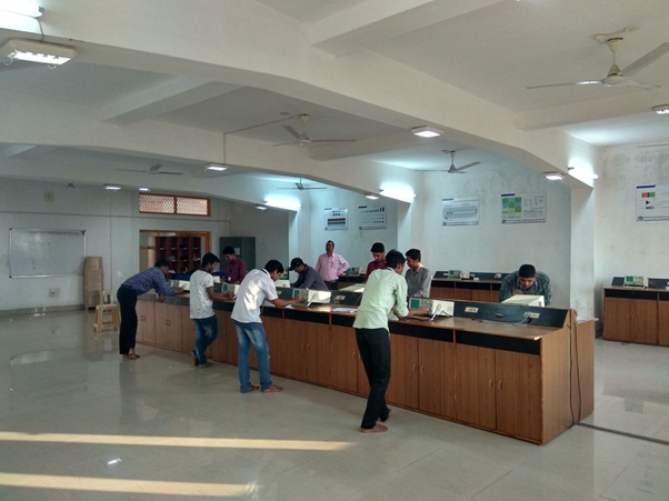
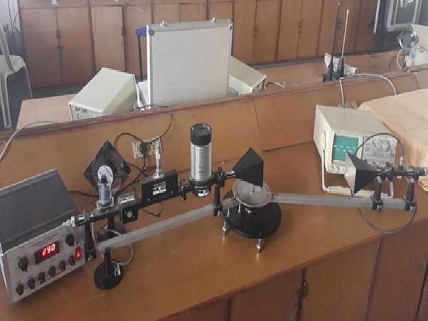
Communication Laboratory is one of the research laboratory for advanced wireless communication.
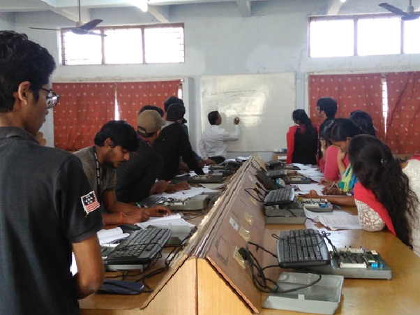
200 hours summer skill development courses in different electronic domains.
4 National Conferences (NCDC) to provide a technical environment to the young researchers in different domains each year.
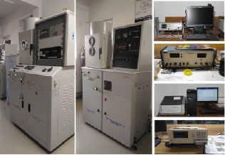
NIST Device Laboratory is commissioned within the Department of Electronics and Communication engineering. The lab has excellent research facilities to conduct experimental research in the field of Nano Science and Engineering for the B.Tech, M.Tech as well as Ph.D students under the guidance of expertise faculties. The research area spans widely from basic semiconductor research to developing semiconductor based devices, material research for finding advanced alternative materials for device applications, sensor modules for futuristic applications and renewable energy and future solar cells. The lab has capability for high quality thin film growth/deposition (oxidation furnace, rf and DC sputtering, Vacuum evaporator), thin film coating (spin coater), film characterization (UV VIS Spectroscopy, Photo luminescence, Four probe, STM) as well as device characterization (LCR meter, IV meter). Each and every year, a mass number of students successfully complete their B.Tech and M.Tech projects in the areas like MOS and MIM capacitor fabrication and characterization, RRAM, fabrication of sensor devices and prototypes, experimental solar cells etc.