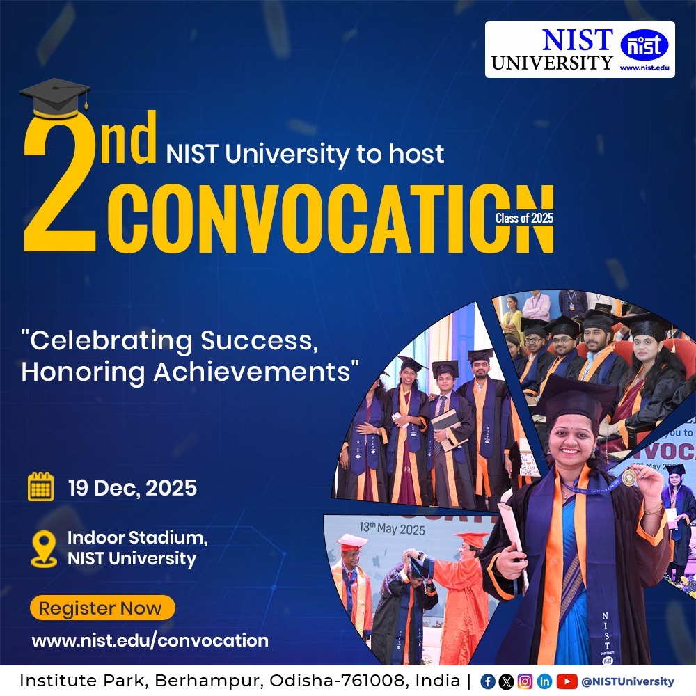
2nd Convocation of NIST University The 2nd Convocation of NIST University, Odisha will be held on Friday, 19th December 2025 at the Indoor Stadium, NIST University, Institute Park, Berhampur. Dr. Hari Babu Kambhampati, Hon’ble Governor of Odisha has graciously consented to preside over the Convocation. All concerned are requested to kindly attend the ceremony. For details regarding the list of degree recipients, Gold and Silver Medal awardees, and the Convocation Programme Schedule, please visit the University website.
Provisional Selection for Ph.D. Admission 2025.
The list of candidates provisionally selected for admission into the Ph.D. Program 2025 of NIST University, as notified vide Office Notification No. NIST/REG/PhD/170/2025 dated 05.07.2025, is hereby published. The selected candidates are placed in order of merit across various departments.
All provisionally selected candidates are required to complete the admission process at the Admission Cell, NIST University, from 24th November to 26th November 2025 during official working hours. Failure to take admission within the stipulated dates will result in cancellation of candidature without further notice. The department-wise merit list of selected candidates is attached for reference.

NIST University is pleased to announce the Counseling & Admission Schedule for the B. Pharmacy program for the academic year 2025-26. The online application process will be open from 25th September 2025 (10:00 am) to 15th October 2025 (6:00 pm), which candidates can complete conveniently from home. The online entrance examination is scheduled for 18th October 2025, followed by the result declaration on 19th October 2025. Selected candidates are required to complete the physical reporting at the University Campus from 22nd October 2025 (10:00 am) to 25th October 2025 (5:00 pm), including Sunday, during working hours (10:00 am – 5:00 pm).

NIST University in collaboration with Army Air Defence College, Gopalpur, is proud to announce the International Conference on Air Defense and Security (ICADS-26), scheduled for 9th & 10th January 2026. This prestigious forum will bring together researchers, industry experts, defense professionals, policymakers, and academicians to deliberate on the latest innovations and challenges in the field of Air Defense and Security. The conference will feature keynote sessions, paper presentations, tutorials, and discussions on emerging areas such as Cyber Warfare, C4ISR Systems, AI/ML applications in threat detection, UAV Countermeasures, Aerospace Sensors, Missile Defense, and Avionics Security. ICADS-26 aims to create a vibrant platform for knowledge exchange, collaboration, and future-ready solutions that address national and global security challenges. Accepted papers will be published in the conference proceedings, with publication in IEEE Xplore (pending approval).
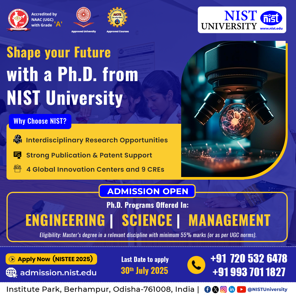
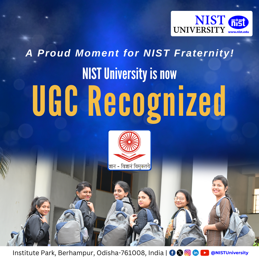
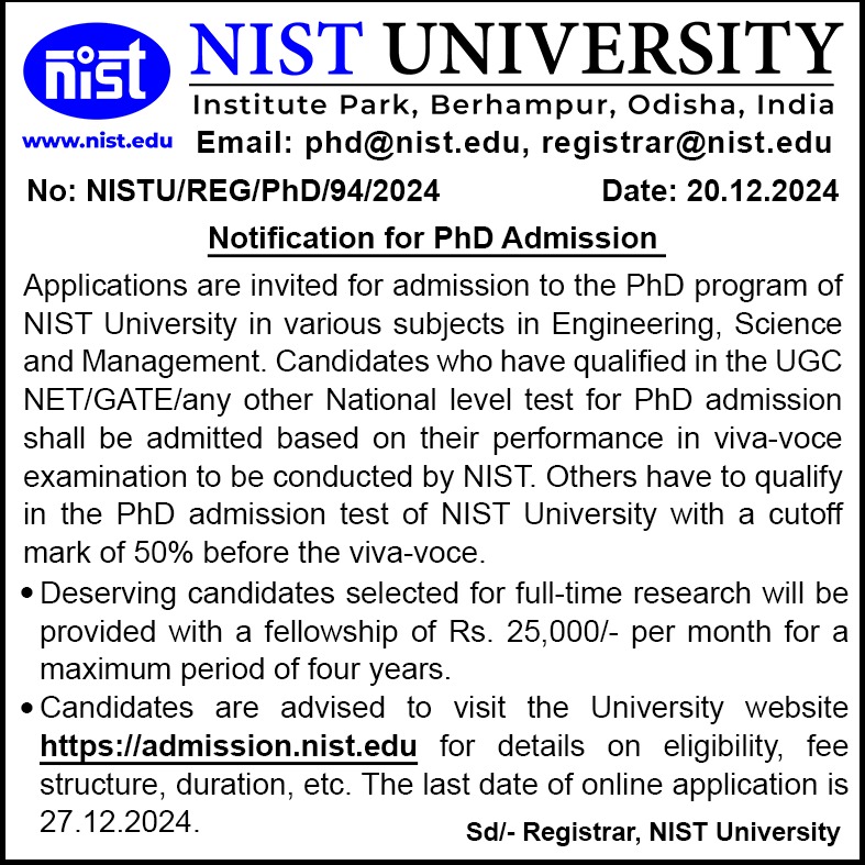
Applications are invited for the Ph.D. programs in Engineering, Sciences, and Management. NIST offers a dynamic research environment with interdisciplinary opportunities, guided by expert faculty and strong mentorship. Our scholars benefit from robust publication and patent support, along with access to 4 Global Innovation Centers and 9 Centers for Research Excellence (CREs). Eligible candidates must hold a Master’s degree in a relevant discipline with at least 55% marks, as per UGC norms.


 (1)-Photoroom.png "For engineering and management programs")