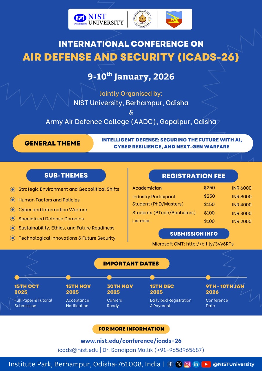
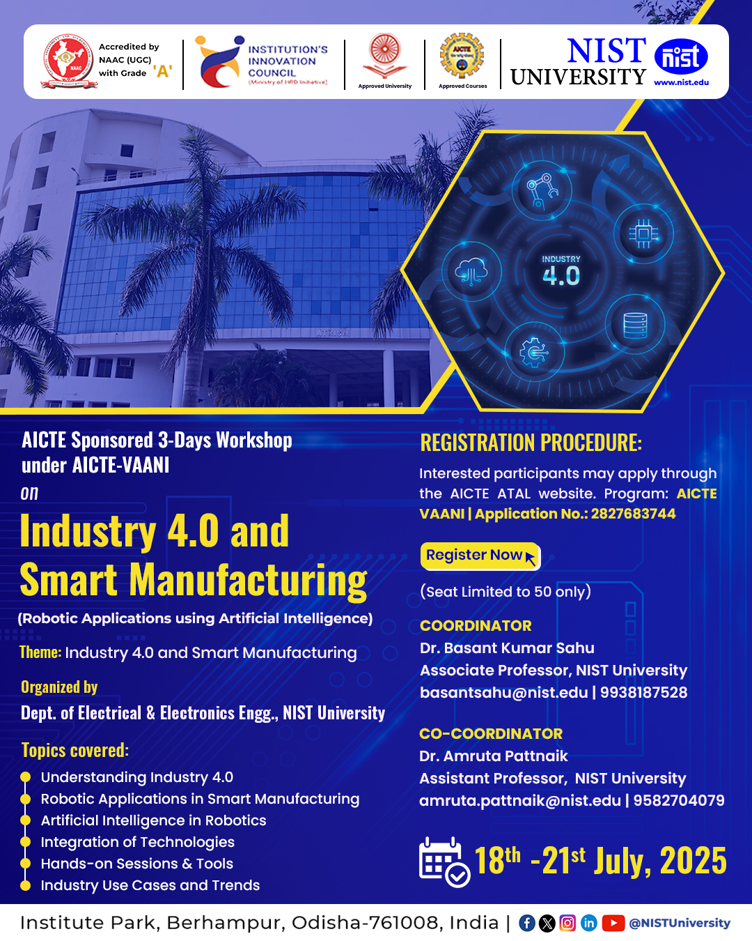
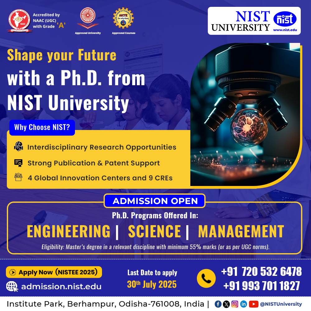
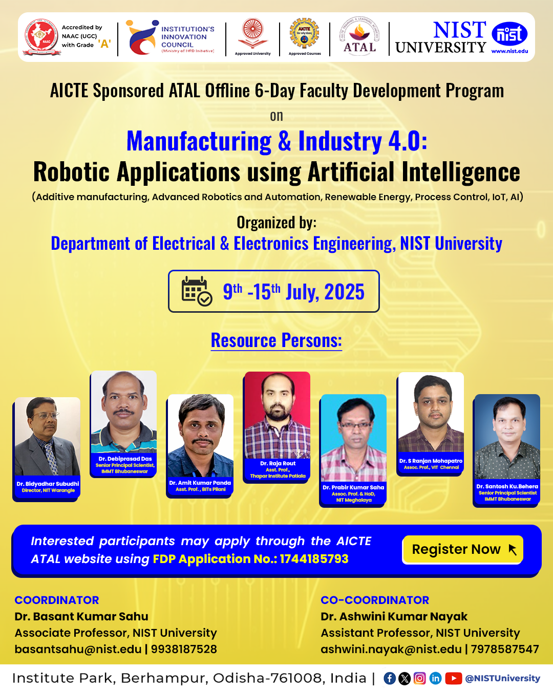
-
M Suresh, Ajit Kumar Panda, Mukesh Kumar Sukla, Jayshree Acharya, Lusita Sahu . M. Suresh, Ajit Kumar Panda, âPower Analysis and Simulation of Low Power Gated-Clock Design of LFSR using 250nm Technologyâ, International Journal of Computational Intelligence Research and Applicationsâ, Vol. 3, No. 1, January â June 2009, pp. 157-161, ISSN: 0973-6794.
-
M Suresh, Mukesh K Sukla, A K Panda, âPerformance Analysis of Multiplexer using Low Power Techniques â, Indian Journal of Scientific Research, 17(2):65 â 73, 2018, ISSN: 0976 â 2876(Print), ISSN: 2250-0138(online).
-
International Conference on VLSI and Communication 2009 (ICVCom-09), SAINTGITS College of Engineering, KERALA.
-
11th IEEE VLSI Design And Test Symposium held at Saha Institute of Radio Physics, Kolkata during August 8-10, 2007.
-
Cadence Userâs Conference âCDN Live â 2018â organized by CADENCE PVT. LTD. at Park Plaza, Bangalore on 06th and 7th September, 2018
-
Participated in the 21st International Symposium on VLSI Design and Test (VDAT-2017) held at Department of Electronics and Communication Engineering, IIT-Roorkee during 29th June â 2nd July. 2017.
-
Participated in 6th Annual Conference of Telemedicine Society of India (TSI), Odisha Chapter (ODITELECON-2017) held on 9th April, 2017 at NIST-Berhampur.
-
Attended Cadence University Conference â Architecture to Silicon to System: Academiaâs Role in Electronic Design and R&Dâ held on December 06, 2016 at Bangalore.
-
Cadence Userâs Conference âCDN Live â 2015â organized by CADENCE PVT. LTD. at Park Plaza, Bangalore on 18th and 19th August, 2015.
-
19th International Symposium on VLSI Design and Test (VDAT 2015), 26TH â 29TH June, 2015 organized by VLSI Society of India and Institute of Technology, Nirma University, Ahmedabad.
-
17th International Symposium on VLSI Design And Test (VDAT 2013) from July 27 â 30, 2013 at Malaviya National Institute of Technology, Jaipur, INDIA.
-
National Conference on VLSI Design & Embedded Systems (NCVDES â 2011), organized by IETE â Pilani Centre in association with CSIR â CEERI, Pilani, BITS â Pilani, Pilani and BKBIET, Pilani at CSIR â CEERI Pilani, Rajasthan, October 12 â 14, 2011.
-
IEEE EDS Mini-Colloquium on âNano Electronicsâ organized by National Institute of Science and Technology, Berhampur, Odisha on 30th December, 2010.
-
Mukesh Kumar Sukla, Shasanka Sekhar Rout, Sunil Kumar Behera, âDesign of Low Power Analog Multiplexer for Sensor Interfacingâ 5th National Conference on Devices and Circuits, 2nd March, 2019, ISBN: 978-93-83060-12-2, PP. 62 - 66.
-
Manoja Kumar Senapati, Mukesh Kumar Sukla, Subhadeepta Tripathy, Rohit Padhy, âDesign and Implementation 8-bit soft-core Microcontroller on FPGAâ 4th National Conference on Devices and Circuits, 24th February, 2018, ISBN: 978-93-83060-16-0, PP. 86 â 91.
-
Abinash Ku Pala, M Suresh, Ajit Ku Panda, Mukesh Ku Sukla, âEfficient Design of 4X4 Vedic Multiplierâ 3rd National Conference on Devices and Circuits, 7th March, 2017, ISBN: 978-93-83060-18-4, PP. 115 â 118.
-
Mukesh Kumar Sukla, M Suresh, âDesign of GDI & Hybrid Adder in Error Tolerant Multiplier for Low Power, High Speed DSP Applicationsâ 2nd National Conference on Devices and Circuits, 19th February, 2016, ISBN: 978-93-82208-78-5, PP. 93 - 97.
-
Niteesh Kumar, Lalit Mohan Upadhyay, M K Sukla, âPhysical Design and Verification of High Precision Sense Amplifier for RAMâ, 1st National Conference on Devices and Circuits, 21st February, 2015, ISBN: 978-93-82208-75-4, PP. 118 - 121.
-
Spandana Gannavarapu, Shyama Nayak, M K Sukla, âImplementation and Verification of I2C Protocolâ, 1st National Conference on Devices and Circuits, 21st February, 2015, ISBN: 978-93-82208-75-4, PP. 67 - 69.
-
Reetish Pattnayak, Rakesh Sahu, M K Sukla, âPower Efficient Pipelined Reconfigurable Fixed-Width Baugh-Wooley Multipliersâ, 1st National Conference on Devices and Circuits, 21st February, 2015, ISBN: 978-93-82208-75-4, PP. 104 - 107.
-
Mithun Kumar Swain, Mukesh Kumar Sukla, âDesign and Implementation of Fast Carry FA for DSP Applicationsâ, 1st National Conference on Devices and Circuits, 21st February, 2015, ISBN: 978-93-82208-75-4, PP. 113 - 117.
-
Meraj Saheel, M. Suresh, A K Panda, M K Sukla, âDesign of Reversible Logic Gates Using 0.12µm Technologyâ, 1ST National Conference on Electronics Communication & Instrumentationâ, e-Marathon 2 â 3 April, 2010.
-
M Suresh, Ajit Kumar Panda, M K Sukla, Madhusmita Mahapatra, Sisira Kanta Panda, Jagannath Satapathy, Meraj Saheel, âDesign of Arithmetic Circuits using Reversible Logic Gates and Power Dissipation Calculation â, International Symposium on Electronic System Design, 978-0-7695-4294-2/10, 2010 IEEE, pp. 85 â 90.
-
Three Day Workshop on âVLSI and Embedded System Design (VESD-2017)â on 13th â 15th October 2017 at the School of Electrical Sciences, IIT-Bhubaneswar, Odisha, INDIA.
-
Two Days workshop on Innovative Research in Pedagogy for Mini-MOOCs Blended with Instruction Strategies to enhance quality of higher education held on 19th â 20th August, 2017 at NIST-Berhampur in collaboration with Thapar University, Patiala.
-
Tutorial Session in the 21st International Symposium on VLSI Design and Test (VDAT-2017) held at Department of Electronics and Communication Engineering, IIT-Roorkee during 29th June 2017.
-
Participated in a Two-Weeks ISTE STTP on CMOS, Mixed Signal and Radio Frequency VLSI Design conducted by IIT-Kharagpur from 30th January to 4th February, 2017 held under the National Mission on Education through ICT (MHRD) at NIST Berhampur (Nodal Center)
-
A Short term course on VLSI Digital Signal Processing Architecture (VDSPA-2017) at School of Electrical Sciences, IIT-Bhubaneswar during 2nd â 6th January, 2017.
-
Attended an FDP on ASIC Verification by MAVEN SILICON, Bangalore on 3rd â 4th September, 2016
-
Attended Workshop on CADENCE and ANYSYS HFSS TOOL TRAINING conducted by Biju Patnaik University of Technology, Odisha at CET Bhubaneswar during 1st â 5th February, 2016.
-
One day tutorial âSCL 180nm CMOS Foundry: High Reliability ASIC Design for Aerospace Applicationsâ at 19th International Symposium on VLSI Design and Test, VDAT 2015 jointly organized by VLSI Society of India and Institute of Technology, Nirma University, Ahmedabad.
-
One day workshop âCadence VLSI Design Toolsâ at 19th International Symposium on VLSI Design and Test, VDAT 2015 jointly organized by VLSI Society of India and Institute of Technology, Nirma University, Ahmedabad.
-
Attended the National Workshop on Embedded Design Flow using XILINX ZYNQ SOC organized by IEEE ED-NIST Student Chapter at NIST-Berhampur in association with CoreEL Technologies and XILINX on 9th â 10th April, 2015.
-
Two weeks workshop on âReal Time Embedded System Design for Signal Processing Application â An FPGA Design Approachâ jointly organized by IEEE EDS NIST Students Chapter and National Institute of Science and Technology, Berhampur, Odisha from 12th â 23rd July, 2013.
-
Two week ISTE Workshop on âAnalog Electronicsâ conducted by Indian Institute of Technology, Kharagpur from 4th â 14th June, 2013 under the National Mission on Education Though ICT (MHRD).
-
1ST Industry Academia Workshop on 11TH and 12TH January 2013 at BVB College of Engineering and Technology, Hubli.
-
Attended Mission 10X workshop conducted at National Institute of Science and Technology at Berhampur from 20th July to 24th July 2010.
-
Attended a workshop on High Impact Teaching Skills by Dale Carnegie & Associates, Inc. Trainer and WIPRO on 20th and 21st, 2010.
-
Attended an intensive AICTE Sponsored Faculty Development Program on MICROELECTRONICS/ VLSI DESIGN FOR ENGINEERS AND SCIENTISTS conducted by National Institute of Science and Technology, Berhampur during 27th July â 8th August, 2009.
-
Attended AICTE sponsored Faculty Development Program on Advanced Computer Control Of Industrial Process & Automation Engineering held during 6th â 11th July, 2009 at NIST-Berhampur.
-
Real-Time Issues on Power Engineeringâ organized by NIST, Berhampur, Odisha on 11th December 2007.
-
Workshop On Embedded System & DSP-in-VLSIâ conducted at NIT, Rourkela during 5th -6th December 2007.
-
One Day Seminar on VLSI Design Using Tanner Tool at NIST, Berhampur on 5th November 2007.


 (1)-Photoroom.png)